Kurnal
@Kurnalsalts
Maybe Kurnal 也许是Kurnal,也许不是Kurnal 中文/EN(?) Kurnal’s English is Terrible,Use Translator Talking Team in Telegram:https://t.me/+XUBY1kMcR3hkMDk1
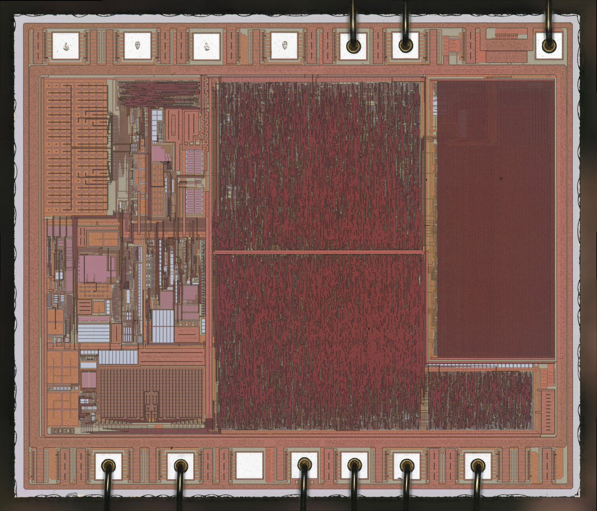
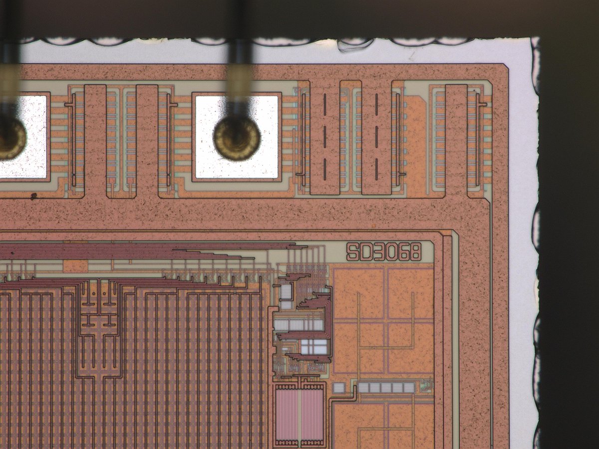
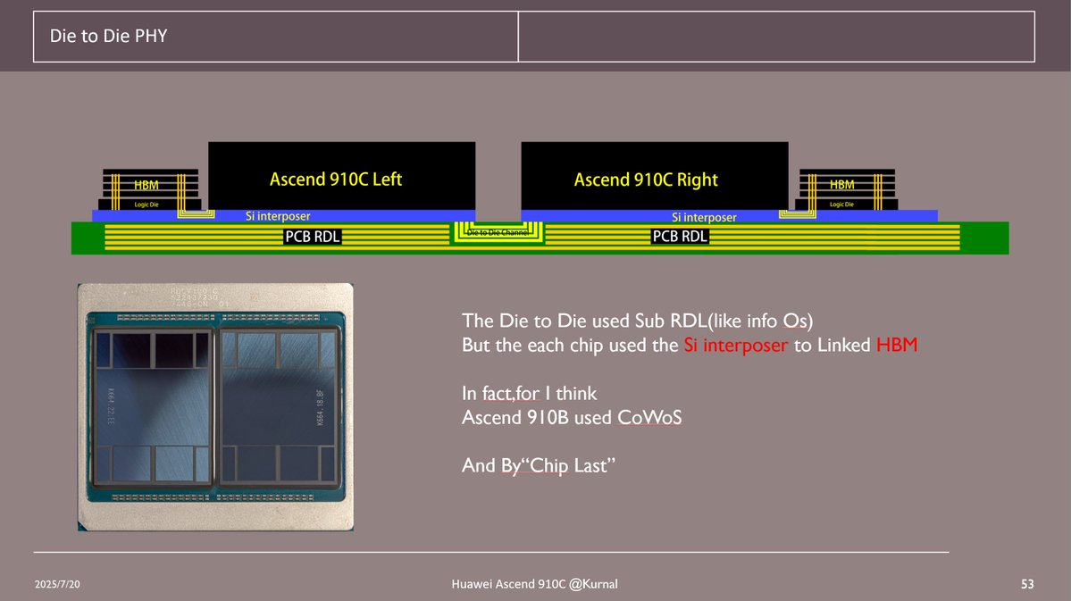
Huawei Ascend 910C chip analyze TSMC N7 Family Same chip with 910B Video on Youtube: youtu.be/0feji7gMrh8?si…
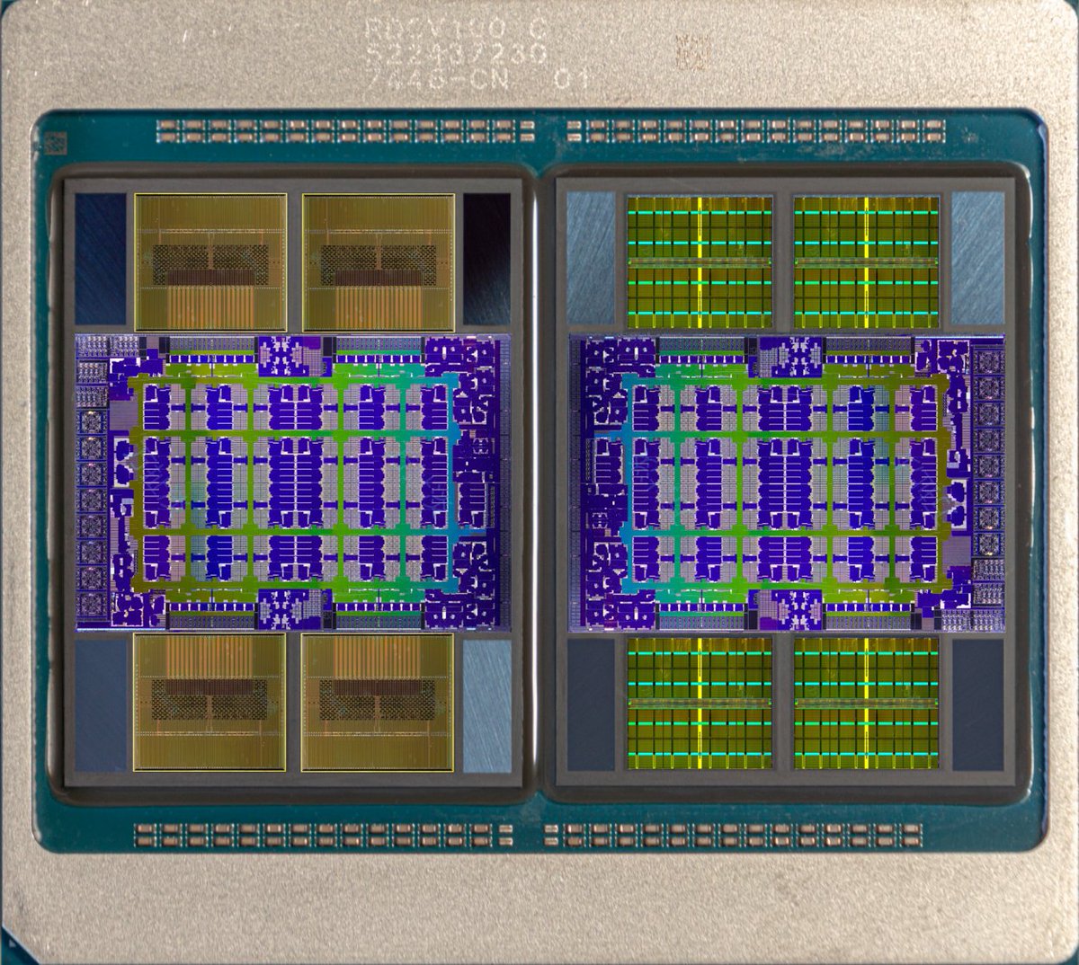
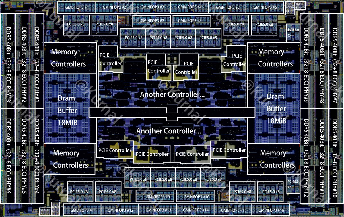
AMD Threadripper 9995WX IOD Dieshot Thanks By@ASUS Tony 俞元麟 give chip Thanks By@万扯淡 Decap @Kurnalsalts Layout P1: IOD Diesize:16.45mm x 25.94mm P2:CPU Diesize:7.76mm x 9.05mm

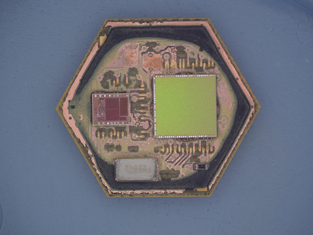
Hexgon Package decaped 2/2 P1:die1 shot P2:die1 diemark P3:die2 shot P4:die2 diemark

working.... New Video: Huawei Car Chip(990A&9610A) analyze Huawei Ascend 910C analyze
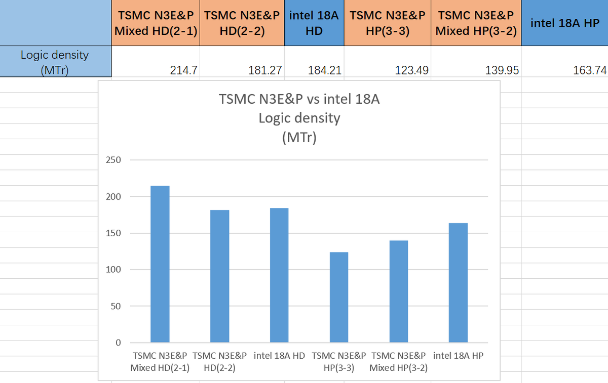
intel3 VS intel 18A HD increase 31.25%,HP increase 33.32% intel18A HD contrast TSMC N3E&P HD 18A HD was similar with TSMC N3E HD(2-2) decrease than TSMC N3E Finflex HD(2-1) 14.2% intel18A HP contrast TSMC N3E&P HP 18A HP have the more density than N3E HP&N3E Finflex HP


lol
2025 VLSI intel 18A analysis (b) 1)Compute Die 114.34mm2 reference other Logic Chip Layout 2)Logic Circuit Area around 46% ~ 52.6 mm2 then scaling 72% 3)SRAM Area around 29% ~ 33.15 mm2 then scaling 12% 4)Total Chip Density scaling approximately 36% ~ 194.98 MTr/mm2
The First SoC by Xiaomi Xring O1 Dieshot Thanks By Geekerwans and 万扯淡 Layout By Kurnal Diesize=10.8x10.6=114.48mm2 Used area=109.5xmm2

Analysis of Xiaomi XRing self-developed watch chip analysis report Video: youtu.be/Q3tDL14_Gd0 bilibili.com/video/BV1DaE6z…


The SWitch2 T239 Analysis Report PDF on Telegam Team: t.me/+DjmQ-kcsAXIyM…
The world's first Nintendo Switch 2 Chip and process analysis report Video: youtube.com/watch?v=uzxA0S…
The world's first Nintendo Switch 2 Dieshot Samsung 8N 8Core A78C,Share 4M L2 1536Cuda/6TPC ampere GPU A detailed process and chip analysis report will be released on Youtube and Bili at 9:30 pm tomorrow. High-resolution photos in Telegram group: t.me/+DjmQ-kcsAXIyM…
Excited to announce our new SemiAnalysis Die Yield Calculator, a tool we made public to help others understand semi yields. Now featuring: Reticle Shot Grid Reticle Graphic New Output Values Notch Support New Yield Models 1/4


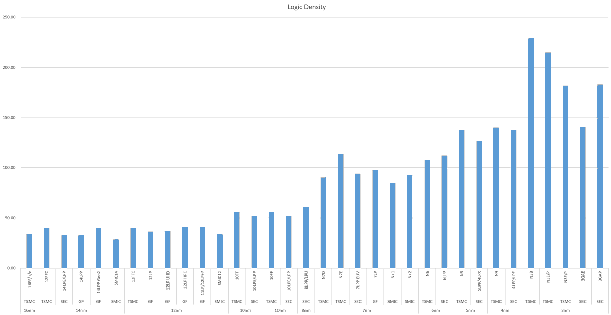
The Semiconductor process with 16nm to 18A Logic Density/mm2 By TSMC/Samsung/Intel/GlobalFound/SMIC

The intel Semiconductor process Total 22nm to 18A Logic density

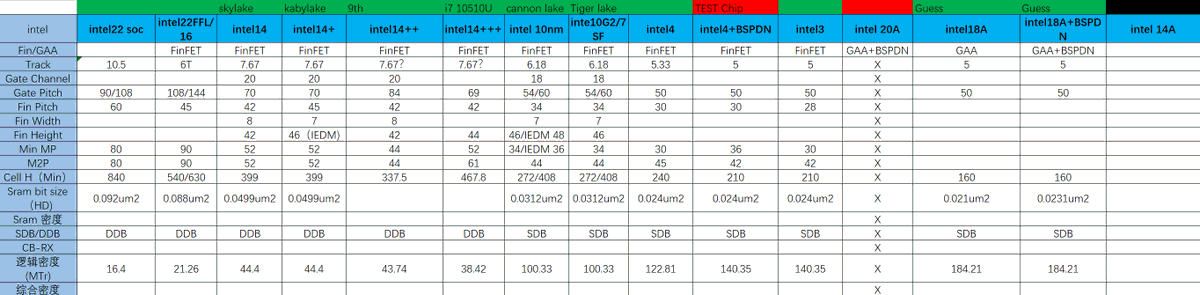
The graph of the 16nm to 3nm(TSMC/SEC/GF/SMIC) Logic density data
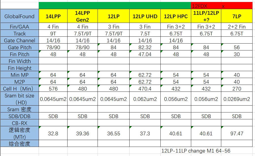
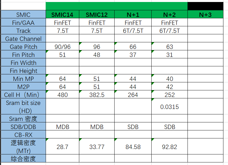
The Global Found and SMIC total 14nm to 7nm Logic Density data P1:Global Found data P2:SMIC data